defects identified and rectified during the electronics assembly
Identifying and rectifying defects during the electronics assembly process is crucial to ensuring the quality, reliability, and performance of electronic devices. This process involves multiple steps and techniques, ranging from initial visual inspections to advanced automated testing. Each step is designed to detect and address potential issues as early as possible to minimize rework and avoid costly failures later in the production cycle.
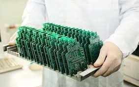
The first line of defense against defects in electronics assembly is visual inspection. This can be performed manually by trained technicians who examine the printed circuit boards (PCBs) and components for visible issues such as misaligned parts, missing components, poor solder joints, or physical damage. To enhance their ability to spot defects, technicians often use magnification tools such as microscopes or magnifying glasses. However, due to the limitations of human inspection, Automated Optical Inspection (AOI) systems are frequently employed. AOI systems use high-resolution cameras and image processing software to automatically scan and detect defects on the PCB, offering high accuracy and consistency in identifying issues.
Once the visual inspection is complete, the next step often involves electrical testing using tools like multimeters and oscilloscopes. Multimeters are used to measure basic electrical parameters such as voltage, current, and resistance, ensuring that components and circuits are functioning correctly. Oscilloscopes allow technicians to visualize and analyze the waveform of signals within the circuit. By comparing these signals to expected patterns, technicians can identify anomalies such as signal distortion, noise, or timing issues, which could indicate underlying defects.
How are defects identified and rectified during the electronics assembly?
In more complex assemblies, In-Circuit Testing (ICT) is a critical technique for identifying defects. ICT uses a bed of nails fixture or flying probe testers to make electrical contact with specific test points on the PCB. This allows for the precise measurement of component values, verification of connections, and detection of issues such as short circuits, open circuits, and incorrect component placements. ICT is particularly valuable because it can quickly test a high volume of boards, making it ideal for mass production environments.
Functional testing is another key method for identifying defects. This type of testing involves simulating the operational conditions under which the electronic device will be used. Functional testers assess the overall performance of the assembly, verifying that it meets its design specifications and performs its intended functions. This testing can reveal defects that might not be apparent through other methods, such as software bugs or issues arising from the interaction between components.
Thermal imaging is an advanced technique used to identify defects related to heat generation. Thermal cameras can detect hot spots on the PCB, which may indicate components that are overheating due to excessive current draw, poor thermal management, or short circuits. By visualizing the thermal profile of the assembly, technicians can pinpoint and address these issues before they cause further damage or failure.
X-ray inspection is another sophisticated method used to identify hidden defects, particularly in solder joints and components that are not visible from the surface. X-ray machines can reveal internal issues such as voids in solder joints, misaligned pins, and internal cracks within components. This is especially important for Ball Grid Array (BGA) packages and other surface-mount devices where traditional inspection methods fall short.
Once defects are identified, rectification involves a combination of rework and repair techniques. For instance, faulty components may be desoldered and replaced with new ones. Tools like soldering irons, hot air rework stations, and desoldering pumps are commonly used in this process. For issues like poor solder joints, technicians can reflow solder to ensure a proper electrical and mechanical connection. Additionally, software updates or firmware revisions might be applied to rectify defects related to the device’s operation.
In conclusion, identifying and rectifying defects during the electronics assembly process is a multifaceted approach involving various inspection and testing techniques. From visual inspections and electrical measurements to advanced methods like ICT, functional testing, thermal imaging, and X-ray inspection, each step plays a crucial role in ensuring the final product’s quality and reliability. Through meticulous defect identification and effective rectification, manufacturers can produce high-quality electronic devices that meet stringent performance standards.